
Table of Contents
What Is Scanning Electron Microscopy?
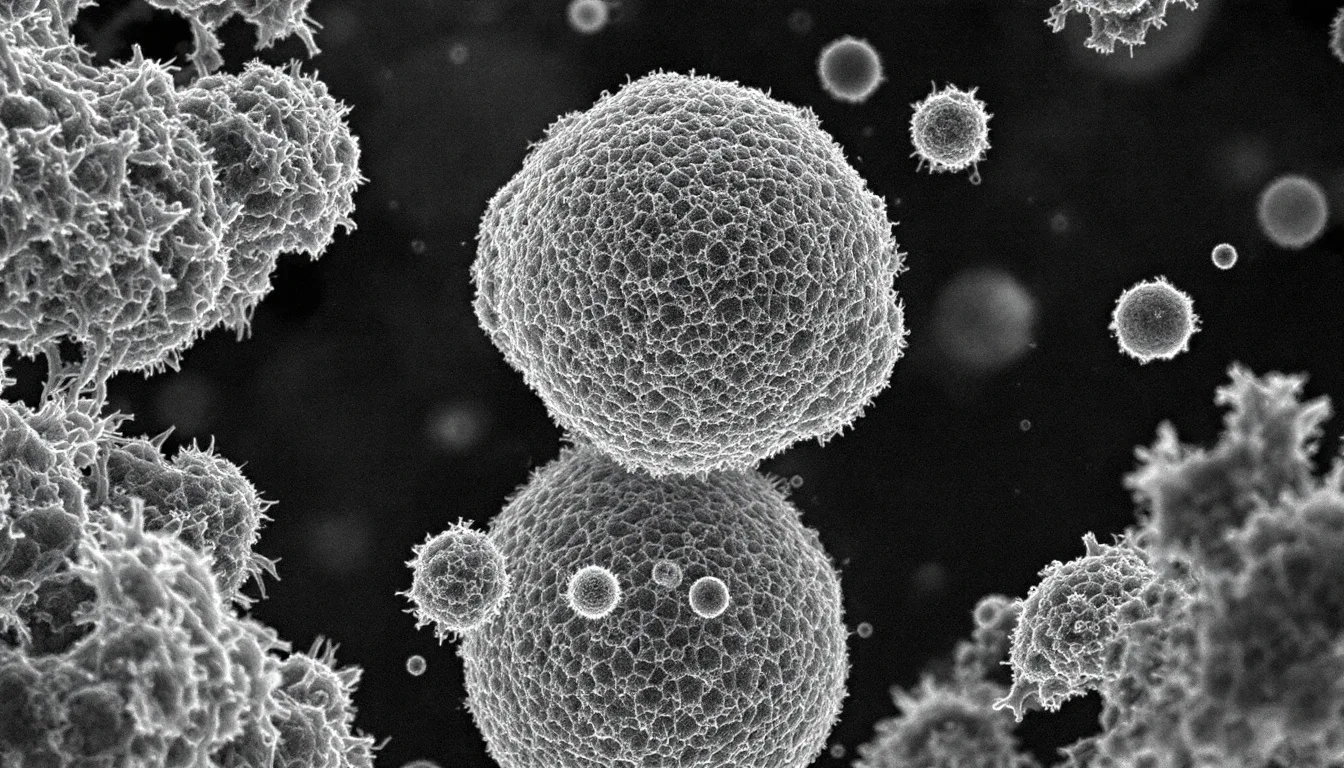
Scanning electron microscopy (SEM) is an imaging technique that uses a focused beam of electrons to scan across a sample’s surface, producing highly detailed images of its topography and composition at magnifications up to 500,000x and resolutions as fine as 1 nanometer. Unlike optical microscopes that use light and glass lenses, SEM uses electrons and electromagnetic lenses, bypassing the fundamental resolution limit of visible light (about 200 nanometers) and revealing a world of surface detail invisible to any conventional microscope.
Since its commercial introduction in 1965, SEM has become one of the most widely used analytical instruments in science and industry. There are an estimated 50,000+ SEMs operating worldwide, used in fields from materials science and semiconductor manufacturing to forensic investigation and art conservation.
Why Electrons Instead of Light?
Here’s the fundamental problem with optical microscopes: light has a wavelength between about 400 and 700 nanometers (depending on color). You physically cannot resolve features smaller than roughly half the wavelength of the light you’re using. Even a perfect optical microscope with flawless lenses hits this wall at around 200 nm. That’s about the size of a small bacterium—plenty for looking at cells, but useless for seeing the nanoscale world of viruses, crystal structures, or semiconductor features.
Electrons, when accelerated through a voltage of 10-30 kilovolts (typical SEM operating conditions), have wavelengths on the order of 0.01 nanometers. That’s roughly 50,000 times shorter than visible light. In theory, this should allow resolution 50,000 times better than optical microscopes. In practice, lens imperfections and other factors limit SEM resolution to about 1-10 nm—still 20-200 times better than the best light microscope. And that’s more than enough to image individual nanoparticles, crystalline grain boundaries, and features on integrated circuits.
How SEM Actually Works
The principle is straightforward even if the engineering is extraordinarily precise. An SEM generates a fine beam of electrons, focuses it to a tiny spot on the sample surface, and then rasters that spot across the surface in a grid pattern—like how an old CRT television painted an image line by line. At each point, the beam interacts with the sample and produces various signals that detectors collect. The intensity of these signals, mapped to each point in the scan pattern, creates the image.
The Electron Gun
At the top of the SEM column sits the electron source. Three types are common:
Thermionic tungsten filaments are the simplest and cheapest. A V-shaped tungsten wire is heated to about 2,700 K (glowing orange-hot) until electrons boil off the surface through thermionic emission. These emitters are inexpensive ($20-$50 per filament) and reliable but produce a relatively large electron source, limiting resolution. Filament lifetime is typically 40-100 hours.
Lanthanum hexaboride (LaB6) emitters are brighter than tungsten—they produce more electrons from a smaller area. A small LaB6 crystal is heated to emission temperature. Better brightness means better resolution, but LaB6 emitters cost $500-$1,000 and are more sensitive to vacuum conditions.
Field emission guns (FEG) are the high-performance option. A very sharp tungsten tip (radius less than 100 nm) in a strong electric field emits electrons through quantum tunneling. The source is incredibly small and bright, producing the finest beams and best resolution—typically 1-3 nm. Cold FEG sources operate at room temperature; Schottky FEG sources use moderate heating combined with field emission. These emitters last thousands of hours but require ultra-high vacuum (10^-9 Pa or better) and cost significantly more.
The electron gun also includes a Wehnelt cylinder or extraction anode that shapes and accelerates the electrons, typically to energies of 0.5-30 keV.
The Electromagnetic Lenses
Glass lenses don’t work for electrons—electrons pass right through glass. Instead, SEM uses electromagnetic lenses: coils of wire that create precisely shaped magnetic fields to bend and focus the electron beam. Just like a glass lens bends light through refraction, a magnetic field bends the path of a moving charged particle through the Lorentz force.
A typical SEM has two or three condenser lenses that narrow the beam diameter and control beam current (how many electrons hit the sample per second), plus an objective lens near the bottom that performs final focusing. The beam spot on the sample is typically 1-10 nm in diameter for a field emission instrument—a spot smaller than most viruses.
Alignment and stigmation corrections (using additional small magnetic coils) ensure the beam is circular and precisely centered. Poorly aligned lenses create elliptical or smeared beam spots that degrade image quality. SEM operators spend significant time on alignment, particularly when first starting up or after changing operating conditions.
The Scan Coils
Between the condenser and objective lenses, electromagnetic scan coils deflect the beam in X and Y directions, steering it across the sample in a raster pattern. The scan speed, area, and number of lines determine the magnification and image quality. Higher magnification simply means scanning a smaller area. Slower scans with more averaging produce cleaner images but take longer—a high-quality SEM image at high magnification might require 30-60 seconds of scan time.
The Sample Chamber and Vacuum System
The sample sits in a chamber maintained at high vacuum—typically 10^-3 to 10^-5 Pa (about a billionth of atmospheric pressure). The vacuum is essential for two reasons: air molecules would scatter the electron beam before it reached the sample, and the electron gun requires vacuum to function.
Most SEMs use a combination of mechanical roughing pumps and either turbomolecular or diffusion pumps to achieve operating vacuum. Pump-down from atmosphere takes 5-20 minutes depending on the system and sample.
The sample is mounted on a motorized stage that provides movement in X, Y, Z (height), tilt, and rotation. Modern stages position the sample with sub-micrometer precision. Some stages include heating (up to 1,000C) or cooling (down to liquid nitrogen temperatures) for in-situ experiments.
The Signals: What You Actually Detect
Here’s where SEM gets really interesting. When the electron beam hits the sample, it doesn’t just bounce off like a billiard ball. The beam electrons interact with the sample atoms in multiple ways, producing several different signals simultaneously. Each signal carries different information about the sample.
Secondary Electrons (SE)
Secondary electrons are low-energy electrons (less than 50 eV) knocked out of the sample atoms by the incident beam. Because of their low energy, they can only escape from the top 1-10 nm of the surface. This makes them exquisitely sensitive to surface topography—edges, bumps, holes, and surface roughness all affect how many secondary electrons escape and reach the detector.
Secondary electron images are what make SEM famous. They have that striking three-dimensional quality that looks almost like a black-and-white photograph taken under dramatic lighting. The Everhart-Thornley detector—positioned to one side of the sample—creates this effect by collecting more electrons from surfaces facing toward it (bright) and fewer from surfaces facing away (dark). Your brain interprets the resulting brightness variations as depth, just as it does with shadows in daily life.
Backscattered Electrons (BSE)
Backscattered electrons are high-energy beam electrons that bounce back after deep interactions with sample atoms. Heavier atoms (higher atomic number) scatter more electrons back, so BSE images show compositional contrast: areas with heavier elements appear brighter. This is incredibly useful for identifying different phases or constituents in a sample. In a polished cross-section of an alloy, BSE imaging instantly reveals the distribution of different metallic phases without any staining or special preparation.
BSE come from deeper in the sample (10-100 nm depth) and a larger volume than SE, so BSE images have lower spatial resolution. But the compositional information they provide is often more valuable than topographic detail.
X-rays (Energy-Dispersive Spectroscopy)
When beam electrons knock inner-shell electrons out of sample atoms, outer-shell electrons fall into the vacancies and release characteristic X-rays. The energy of these X-rays is unique to each element—like an elemental fingerprint. An energy-dispersive spectrometer (EDS or EDX) mounted in the sample chamber collects these X-rays and identifies which elements are present and roughly how much of each.
EDS turns the SEM from an imaging tool into an analytical instrument. You can map the elemental composition across a sample with sub-micrometer spatial resolution. Where is the carbon concentrated? Is that bright particle in the BSE image titanium or zirconium? EDS answers these questions quantitatively.
Chemistry departments lean heavily on SEM-EDS for materials characterization, phase identification, and quality control. The combination of morphological imaging (SE), compositional imaging (BSE), and elemental analysis (EDS) from a single instrument makes SEM the Swiss Army knife of materials analysis.
Other Signals
Cathodoluminescence (CL): Some materials emit visible light when struck by electrons. CL imaging reveals crystal defects, dopant distributions in semiconductors, and mineral phases in geological samples.
Electron backscatter diffraction (EBSD): Electrons scattered by the crystal lattice create diffraction patterns that reveal crystal structure, grain orientation, and texture. EBSD has become essential for metallurgical analysis and computational biology applications involving biomineralization.
Specimen current: Electrons absorbed by the sample create a measurable current that provides yet another contrast mechanism.
Sample Preparation
This is the unglamorous but critically important part of SEM work. Garbage in, garbage out—and with SEM, “garbage” includes contamination, charging, and artifacts that can be invisible to the naked eye.
Conductivity and Charging
Here’s a practical problem: the electron beam deposits charge on the sample surface. If the sample is electrically conductive (metals, most alloys), this charge dissipates through the ground connection. No problem. But if the sample is non-conductive (polymers, ceramics, biological tissue, most geological minerals), charge accumulates on the surface. This creates electric fields that deflect the beam and distort the image—bright streaks, image shift, and contrast anomalies that make the image useless.
The standard solution is coating the sample with a thin (5-20 nm) layer of conductive material. Gold and gold-palladium alloy are traditional choices—they’re easy to deposit by sputter coating (a simple vacuum process) and produce excellent SE images. Carbon coating is preferred for samples that will undergo EDS analysis, because gold’s X-ray peaks can interfere with elemental identification.
Variable-pressure SEM (VP-SEM) and environmental SEM (ESEM) offer alternatives. By operating at slightly higher chamber pressure (1-2,600 Pa), gas molecules in the chamber help neutralize surface charge. This allows imaging of uncoated, non-conductive samples—including wet biological specimens—at some cost in resolution.
Biological Sample Preparation
Cell biology and biological sciences present the greatest sample preparation challenges for SEM. Living tissue is mostly water, and water boils explosively in vacuum. The standard protocol for biological SEM involves:
- Chemical fixation with glutaraldehyde and/or osmium tetroxide to cross-link proteins and preserve structure
- Dehydration through a graded series of ethanol concentrations (30%, 50%, 70%, 90%, 100%)
- Critical point drying or freeze-drying to remove ethanol without the surface tension forces that would collapse delicate structures
- Mounting and coating for conductivity
Critical point drying uses liquid CO2 to replace ethanol, then raises temperature and pressure above CO2’s critical point (31.1C, 73.8 bar) where liquid and gas become indistinguishable. Slowly venting the pressure transitions the CO2 to gas without ever passing through a liquid-gas boundary—avoiding the surface tension that would destroy fine structures like cell membranes and cilia.
Cryo-SEM is an alternative approach: rapidly freeze the sample (typically by plunging into liquid nitrogen or liquid ethane), fracture it under vacuum, and image the frozen surface. This preserves hydrated structure better than chemical fixation and is faster, but requires specialized cryo-stages and transfer systems.
Cross-Sectioning and Polishing
For internal structure analysis, samples are cross-sectioned, mounted in epoxy resin, and polished to a flat, scratch-free finish. The polishing sequence progresses from coarse grinding (120-400 grit) through increasingly fine abrasives (diamond paste from 6 micron down to 0.05 micron) to produce a mirror finish. Final polishing with colloidal silica reveals microstructure without mechanical deformation artifacts.
Focused ion beam (FIB) instruments can mill cross-sections directly into a sample with nanometer precision. FIB-SEM systems combine ion beam milling with SEM imaging, allowing serial sectioning and 3D reconstruction of sample volumes at nanometer resolution.
Applications: Where SEM Makes a Difference
Semiconductor and Electronics Industry
SEM is arguably the most critical analytical tool in semiconductor manufacturing. Every step of chip fabrication—lithography, etching, deposition, planarization—is monitored by SEM. Critical dimension SEM (CD-SEM) measures feature widths on patterned wafers with sub-nanometer precision. Defect review SEM locates and classifies microscopic defects that could cause chip failure.
Modern logic chips have features as small as 3-5 nm. Only electron beam instruments can resolve these dimensions. The semiconductor industry operates tens of thousands of SEMs worldwide, many running 24/7 in automated inspection modes. Digital signal processing algorithms process SEM images to extract measurements and identify defects automatically.
Materials Science and Metallurgy
SEM reveals the microstructure that determines a material’s properties. Grain size and shape, phase distribution, precipitate morphology, fracture surfaces, corrosion products, coating thickness, weld integrity—all are routinely examined by SEM.
Fractography—the study of fracture surfaces—is perhaps the most dramatically visual SEM application. A fractured metal surface that looks smooth and featureless to the naked eye reveals complex detail under SEM: ductile dimples, brittle cleavage facets, fatigue striations, intergranular cracking, and inclusions that initiated failure. A skilled fractographer can read a fracture surface like a book, reconstructing the stress state, crack propagation direction, and failure mechanism from the SEM images alone.
Forensic Science
Forensic SEM-EDS identifies gunshot residue particles (unique spheres of lead, barium, and antimony), matches paint chips to vehicle sources, analyzes fiber evidence, and examines tool marks. The elemental analysis capability is particularly powerful—it can determine the composition of trace evidence too small to analyze by other methods.
Geology and Paleontology
SEM reveals the microscopic world of rocks, minerals, and fossils. Pollen grains, diatoms, foraminifera, and other microfossils are routinely imaged and identified by SEM. Clay mineral morphology, volcanic ash particle shapes, and sedimentary grain surface textures provide information about depositional environments and geological history.
Art Conservation
Museum conservators use SEM to analyze pigments, binding media, paper fibers, textile weaves, and corrosion products on metal artifacts. Cross-sections of paint layers reveal the artist’s technique and subsequent restorations. EDS identifies the elements in pigments—distinguishing lead white from titanium white, for example—helping to date and authenticate works.
Biology and Medicine
Beyond basic cell biology research, SEM is used to examine tissue scaffolds for regenerative medicine, quality-control medical devices (stents, implants, sutures), and study the structure of biomaterials. Biotechnology researchers use SEM to characterize nanoparticle drug delivery systems, biomaterial surfaces, and bacterial biofilms.
The Limitations You Should Know About
SEM is powerful, but it’s not perfect.
Vacuum requirement: Standard SEM needs high vacuum, which limits what you can image. No liquids, no outgassing samples, no live organisms (unless you use ESEM or cryo-SEM, which have their own limitations).
Conductive sample requirement: Non-conductive samples need coating or variable-pressure conditions, adding preparation steps and potentially obscuring fine surface detail.
Surface-only information: SEM images the surface and near-surface region. It can’t see deep internal structure (that’s what TEM is for, or cross-sectioning plus SEM).
Beam damage: The electron beam deposits energy that can damage sensitive samples. Polymers, biological tissue, and some minerals degrade under electron bombardment—burning, shrinking, or losing volatile components. Operating at lower voltages and beam currents reduces damage but also reduces signal and resolution.
No direct height measurement: Standard SEM images look 3D but are actually 2D projections. True height measurement requires either stereoscopic imaging (two images at different tilt angles) or complementary techniques like atomic force microscopy.
Cost and infrastructure: Even modest SEMs need a stable room (vibration and electromagnetic interference degrade images), reliable vacuum pump maintenance, and trained operators. The instrument itself is a significant capital investment.
Modern Advances
Tabletop and Compact SEMs
Since about 2005, tabletop SEMs have made electron microscopy accessible to smaller labs, schools, and industrial quality control departments. These instruments sacrifice some resolution (typically 15-30 nm) and flexibility for dramatically smaller size, lower cost ($50,000-$150,000), and simpler operation. Some can be operated by non-specialists after minimal training.
Automated and AI-Assisted Analysis
Modern SEMs increasingly incorporate machine learning for automated particle analysis, defect classification, and feature measurement. An SEM can be programmed to scan an entire sample, identify particles of interest based on morphology or composition, classify them, and generate statistical reports—all without human intervention. This is transforming quality control in industries from pharmaceuticals to mining.
Correlative Microscopy
Combining SEM with other techniques—confocal fluorescence microscopy, Raman spectroscopy, atomic force microscopy—on the same sample area provides complementary information that no single technique can deliver. Correlative platforms are becoming standard in advanced research facilities.
In-situ Experiments
Specialized stages allow samples to be heated, cooled, strained, or exposed to reactive gases while being imaged in the SEM. Watching a metal grain grow during heating, a crack propagate under stress, or a catalyst change structure during reaction provides real-time insight into active processes that static images can’t capture.
Getting Access to SEM
If you need SEM analysis, you don’t necessarily need to buy one. University shared instrumentation facilities, government labs (many NIST facilities offer user programs), and commercial analytical service labs all provide SEM access. Typical rates for academic shared facilities are $30-$100 per hour for trained users and $100-$300 per hour for full-service analysis (the operator does everything).
For industrial quality control requiring frequent SEM use, a tabletop SEM may pay for itself in a year or two compared to outsourcing. The newer compact models are designed for operators without extensive microscopy training—automated column alignment, preset imaging conditions, and push-button operation make them practical for production environments.
The Big Picture
Scanning electron microscopy opened a window into a world our eyes can’t see. Before SEM, the surfaces of materials, the shapes of microorganisms, the architecture of fractured metals, and the topography of semiconductor circuits were either invisible or crudely imagined. SEM made them visible with startling clarity and detail.
The iconic SEM images—a fly’s compound eye, a pollen grain’s complex surface, the branching crystallites of a metal fracture—have become part of our visual culture. They remind us that the world at the nanoscale is just as complex, beautiful, and surprising as the world we see with our own eyes. And unlike so many technologies that have come and gone, SEM after 60 years remains indispensable. It’s hard to think of another scientific instrument that serves so many different fields so effectively.
Frequently Asked Questions
How much does a scanning electron microscope cost?
A new SEM ranges from about $50,000 for a basic tabletop model to over $2 million for a high-end field emission instrument with multiple detectors and analytical capabilities. Used and refurbished SEMs can be found for $20,000-$100,000. Operating costs include electricity, cooling water, vacuum pump maintenance, and periodic filament or emitter replacement. Many universities and research institutions offer SEM access as a shared service for $50-$200 per hour.
What's the difference between SEM and TEM?
SEM scans a focused beam across a sample's surface and collects signals from interactions at or near the surface, producing images of surface topography and composition. TEM (transmission electron microscopy) sends electrons through an ultra-thin sample (less than 100 nm thick), creating images of internal structure at atomic resolution. SEM is better for surface features and 3D appearance; TEM provides higher resolution but requires extensive sample preparation.
Can SEM image living cells?
Conventional SEM cannot image living cells because the sample must be placed in a high vacuum, which would instantly kill and dehydrate biological specimens. However, environmental SEM (ESEM) can image samples in low-vacuum conditions with some water vapor present, allowing observation of hydrated biological specimens. Cryo-SEM rapidly freezes samples and images them at very low temperatures, preserving near-native structure.
What magnification can SEM achieve?
SEM magnification ranges from about 10x to 500,000x or more, with practical useful magnification depending on the instrument and sample. Most routine work falls between 100x and 50,000x. Resolution—the ability to distinguish two closely spaced features—is typically 1-10 nanometers for modern field emission SEMs. That's roughly 100-1,000 times better than the best optical microscopes.
Why do SEM images look 3D?
SEM images have a remarkable three-dimensional appearance because of how secondary electrons are detected. Surfaces tilted toward the detector emit more electrons (appearing brighter) while surfaces facing away emit fewer (appearing darker). This creates natural-looking shadows and highlights that your brain interprets as depth and topography—similar to how shadows make objects look three-dimensional in a photograph.
Further Reading
Cite this article
APA
WhatIs.site. (2026). What Is Scanning Electron Microscopy?. Retrieved May 27, 2026, from https://whatis.site/scanning-electron-microscopy MLA
"What Is Scanning Electron Microscopy?." WhatIs.site, March 6, 2026, https://whatis.site/scanning-electron-microscopy. Accessed May 27, 2026. Chicago
WhatIs.site. "What Is Scanning Electron Microscopy?." Last modified May 12, 2026. https://whatis.site/scanning-electron-microscopy. HTML
<a href="https://whatis.site/scanning-electron-microscopy">What Is Scanning Electron Microscopy?</a> — WhatIs.site Related Articles
What Is Chemistry?
Chemistry is the science of matter and how substances interact, bond, and transform. Learn about atoms, molecules, reactions, and why chemistry matters.
scienceWhat Is Cell Biology?
Cell biology is the scientific discipline that studies cells — the basic structural, functional, and biological units of all known living organisms.
technologyWhat Is Biotechnology?
Biotechnology is the application of biological systems, living organisms, or their derivatives to develop products, processes.
scienceWhat Is Computational Biology?
Computational biology is the field that applies mathematical modeling, statistical analysis.
technologyWhat Is Digital Signal Processing?
Digital signal processing (DSP) manipulates signals like audio, images, and sensor data using math and algorithms. Learn how DSP works and where it's used.